


News
iPhone X Teardown P1
Date: 01-22-2018 Click: 11226Video Overview

Step 1 iPhone X Teardown

The iPhone X is here! Here's the fillin' inside that glass sandwich:
A11 "Bionic" chip with neural engine and embedded M11 motion coprocessor
5.8 inch "all-screen" OLED multitouch Super Retina HD display with 2436 × 1125-pixel resolution (458 ppi)
Dual 12 MP cameras (wide-angle and telephoto) with ƒ/1.8 and ƒ/2.4 apertures and OIS
7 MP TrueDepth camera with ƒ/2.2 aperture, 1080p HD video recording, and Face ID
Support for fast-charge and Qi wireless charging
Our A1865 global unit has broad cellular band support as well as 802.11a/b/g/n/ac Wi‑Fi w/MIMO + Bluetooth 5.0 + NFC.
Step 2


The iPhone has come a long way in ten years—so long, in fact, that the design has cycled back a bit, and this iPhone looks more like the original than we've seen in a long time.
Except of course for that camera bump, and shiny stainless steel rim, and glass back, and Lightning connector...
As was the case with the iPhone 8 earlier this year, Apple has banished the unsightly (and environmentally responsible) regulatory markings from the back of the iPhone X.
Jony finally has the featureless smooth backplane you know he's always wanted. Hopefully these phones still make it to recyclers without the hint and don't get dumped in the trash.
Step 3


Before we dive in blindly, let's get some 10-ray X-ray recon from our friends at Creative Electron.
Here's what we found:
Not one, but two battery cells. That's a first in an iPhone!
A super-tiny logic board footprint. Based on the overlaid solder points, it looks like there are two stacked layers.
To make room for the extra front-facing sensors, the earpiece speaker has been shifted down quite a bit.
There's a mysterious chip between the Taptic Engine and lower speaker—we're curious to see what's down there!
Step 4


This pentalobe looks weirdly unfinished. The bottom screws are more like pins if we're honest.
This screw moves the threaded section from the display to the steel frame, and extends the unthreaded section into a freakishly long pin.
Our best guess is that this allows the display a bit of flexibility, while also allowing it to move its mounting bracket toward the interior of the phone, incidentally making room for a beefed-up Lightning connector.
Step 5


Looks like sideways-opening iPhones are here to stay. Apple surprised us with this little trick on the 7 Plus, but by now it's standard.
This single bracket covers every logic board connector—we've never seen this kind of connector density.
And once again, we're faced with tri-point screws standing sentry over any repairs once you get past the pentalobe screws guarding the door.
Something tells us Apple doesn't really want us (or you) tinkering in here.
Step 6


After freeing the massive unibracket from the logic board, we can finally steal a peek at the hardware powering Cupertino's latest flagship.
We'll get a better look at the hardware on the display later, for now we satisfy ourselves with an X-ray—turns out that mystery chip is mounted to the display!
For a change of pace, the display lifts off and leaves the front-facing camera behind.
This body shot confirms the layout we observed in our X-Ray recon: most real estate is occupied by the new dual-cell battery, and the logic board has shrunk significantly.
Step 7


The dual rear camera has a beefy bracket that looks like it might offer some bendgate-proofing support for the delicate components.
The cameras are additionally secured to the rear case with some foam adhesive to keep things from jostling out of place. These cameras really need to stay put for Portrait Mode and similar features to work their magic.
Surrounding the camera housing cover glass, you can see tiny spot welds likely holding the walls of the camera bump to the case.
Step 8
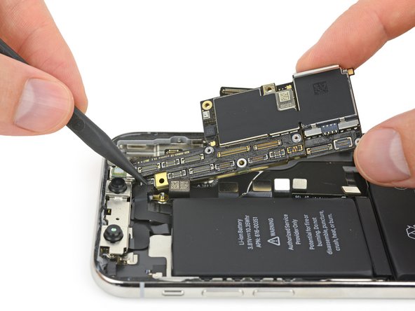

We finally free this most-dense of logic boards to get a closer look.
This miniaturized logic board is incredibly space efficient. The density of connectors and components is unprecedented. Ounce for ounce, even an Apple Watch has more bare board.
The compact iPhone X board manages to pack more tech and still make the iPhone 8 Plus board to its left look gangly and expansive.
Comparing the footprint of the two boards, the iPhone X motherboard is about 70% of the size of the iPhone 8 Plus board—that's a lot more floor space for battery.
Step 9


How did Apple put even more tech in 70% of the footprint? By folding the board in half, of course.
The two halves are soldered together, so we got some help from our hosts Circuitwise and their BGA hot air rework station to separate the layers.
With the pieces separated, we tallied the area of all of the separate layers, and added it up to 135% of the iPhone 8 Plus logic board's area. Way to go putting more into less, Apple.
The iPhone X logic board is the first double-stacked board we've seen in an iPhone since the very first iPhone (third photo).
The downside of this clever design is that board-level repair will be extremely difficult—near impossible in some cases.
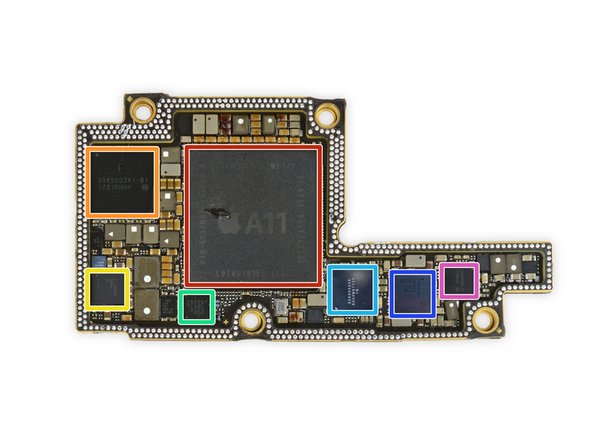

On the first half:
Apple APL1W72 A11 Bionic SoC layered over SK Hynix H9HKNNNDBMAUUR 3 GB LPDDR4x RAM
Apple 338S00341-B1 power management IC
TI 78AVZ81 battery charger
NXP 1612A1—Likely an iteration of the 1610 tristar IC
Apple 338S00248 audio codec
STB600B0
Apple 338S00306 power management IC
Step 11


Apple/Murata USI 170821 339S00397 WiFi / Bluetooth module
Qualcomm WTR5975 gigabit LTE transceiver.
Qualcomm MDM9655 Snapdragon X16 LTE modem and PMD9655 PMIC. But Apple is dual-sourcing the modem, and TechInsights found an Intel XMM7480 (PMB9948) in their A1901 model. Even though the modem is capable of it, Apple isn’t supporting Gigabit speeds with the Qualcomm part.
Skyworks 78140-22 power amplifier, SKY77366-17 power amplifier, S770 6662, 3760 5418 1736
Broadcom BCM59355 wireless charging controller
NXP 80V18 PN80V NFC controller module
Broadcom AFEM-8072, MMMB power amplifier module
Step 12

And on the outside of the logic board sandwich:
Toshiba TSB3234X68354TWNA1 64 GB flash memory
Apple/Cirrus Logic 338S00296 audio amplifier
Step 13


Okay, so Apple made a PCB sandwich, but how does it work?
They created a third spacer PCB that lines the perimeter. And instead of connecting the two layers with a fussy flex cable, data travels along dozens of through-hole vias.
Here, the A11 SoC lies nestled at the center of the main board. You can get a sense of the 3D structure of the board from the X-ray photos. The cylinders around the edge are holes filled with solder connecting the two boards.
